Page requests to the metal - hardware level
This post is part of the page requests to the metal series where we cover all the steps from a web request down to the electrons that move in the CPU, see the intro/overview page to see where this fits in.
We get to the step eventually where we aren't dealing with instructions to do things but get to the point where things are actually taking place on the hardware.
Machine code is perhaps the lowest level of such instructions and is at the level in which it's completely dependent on the hardware that is being run.
At this level of abstraction you can't just take the code an run it somewhere else, as the other hardware will not necessarily have the needed instruction sets to make it work.
How the machine code is executed:
In an abstract sense to perform an addition we have to get a register and fill it with the first number then get another register and fill with second number. Then we must add the contents of the 2 registers before we can return them. How this is represented in opcodes will depend on the hardware. From here on we are assuming the x86 Instruction set architecture 1. Unlike my old colleague Cao I've never wrote any x86 directly to hex files and honestly I don't plan on any time soon :) but here's a window into the type of info you would need to know in order to be able to do that.
Once again using compiler-explorer: https://godbolt.org/g/QZ4aVT
In this you can see the mapping from assembly to the x86_64 hex codes.
Note that on the x86 platform we have a few ways of performing an addition each with their own opcode, see http://x86.renejeschke.de/html/file_module_x86_id_5.html for information on the various addition opcodes.
Here we see that the add opcode is represented in hexadecimal as
01 d0. If we consult our ASCII table (man ascii) we see that this
could also be written as 01 \r which from the documentation linked
above tells us this this opcode performs: "Add r8 to r/m8".
If you are interested in learning more about machine code with x86-64 I would recommend having a look at this course handout.
So how does this actually get executed on the hardware?
Hardware implementation details
From here on in what happens can potentially be very different depending on what machine we are running. This is exactly the issue that "high level programming languages" seeks to shield us from when developing applications that do not intrinsically have any connection with the hardware that they are running on. (The "high" in "high level programming languages" refers to a high level of abstraction from the hardware implementation. Contrast this with say writing a sound card driver where your code is intrinsically tied to specific hardware and cannot be written in such a language)
Outside systems programming, modern software development very rarely has to deal with this level. One of the towering achievements of many of the operating systems we currently use is just how little we need to deal with this level when we are writing our software.
For now we will gloss over the way in which the data is retrieved from RAM, we just will assume that it's in the CPU registers and can be directly accessed. (The mechanisms behind loading items from memory to the CPU cache to registers can be complicated and depends on the CPU architecture, see this section for more detail)
As we saw above we fetch the numbers we need from the registers and then we add them together and pop the result from a register. We instruct the CPU to do these operations by sending binary encoded information which are the opcodes as specified in the instruction set architecture. The CPU then executes these commands accordingly.
But how does the CPU actually execute these instructions?
Microcode:
We are now at the hardware level. There's an interesting step that isn't really that well known (it's been a while since the fDiv bug hit the headlines), to save silicon space on the chips some of the less common instructions are actually implemented in software on the chip which is called microcode.
While implementing microcode might initially seem like a step that would make chips more expensive it's actually quite economical. By approaching chip design this way we get more powerful chips as we save hardware resources on the less common operations we get more silicon available. In the newly freed up space we have more power available to dedicate to more common operations and more silicon space free for fast cache which overall is a win for performance (with the high clock speeds of modern CPUs the speed of fetching data from RAM including the electrical transmission time matters, caches implemented on the same die can be substantially faster). We also get things like the ability to update the microcode on the chip to fix bugs caused by errata in the chip designs.
Going back to the days where there was a clearer divide between RISC vs CISC explains a few things. At one point when people were writing more code in assembly it helped the productivity of the programmers to have more opcodes available that did more complicated operations. For example you might have an opcode for performing a modulo, which is a specific task but might not be a common task. For example when I was programming the firmware on ATMEGA chips some did not have have hardware support for a modulo operation so the C compiler would create that operation from more simple operations (this was really slow though). Having a specific opcode for a modulo that was fast would have been very convenient for me. Having an opcode for every possible instruction is not the most efficient approach when considering the proliferation of compiled high level languages. For example that code I wrote on the ATMEGA could implement the modulo anyway so taking up valuable silicon for that opcode would take away power from something else (or add to the cost of the chip).
x86 chips is definitely a CISC architecture as the x86 instruction set is large. The original chips would have directly implemented these opcodes in dedicated silicon. As time has gone on more code is being written in high level languages and less in assembly. Compared with the compilers that existed at the birth of x86 current optimizing compilers for modern high level languages are really good at optimizing stuff and happen to make machine code that's mostly just basic operations. Hardware design has followed these developments in the software world and RISC is the dominant architecture as a result in most modern desktops/servers. However the x86 family is designed with very large amount of care put into maintaining backwards compatibility with older processors. You can run really old x86 code on a modern say Intel i7 or whatever, which is truly remarkable since a lot has happened in the intervening years and yet older code will still run on newer processors. If you send any x86 opcode to the chip it will get processed, the most common opcodes are implemented directly in the fastest paths of the silicon, but the slower more complex opcodes are translated into simpler operations for execution in the CPU itself. Essentially there's a RISC core in the new x86 chips which maintains the support for all the CISC operations by a translation step on the chip itself.
Some operations can be computed directly like adding 2 registers. This is a very common operation and is implemented directly in dedicated silicon. Less common operations such as taking the inverse tangent of a number might have their own opcode (depending on the hardware system) but might not have their own dedicated silicon. Essentially the microcode is an interpreter in the chip that determines how the opcodes will be executed on the chip. It's cheaper and more efficient from a silicon point of view to not dedicate too much chip surface area to uncommonly used operations because that surface area takes away from having more power for the more common operations/cache/etc. In this case we have a simple addition so lets say the whole thing is executed directly on the silicon via fast circuitry.
Because the x86 microcode isn't open source we are forced to gloss over this step here. If you are interested in this step you might be interested in some attempts people have made at reverse engineering this:
- Breaking the x86 ISA
- Reverse Engineering x86 Processor Microcode
- A history of creative x86 virtual memory uses
Processor pipeline
Most modern CPUs execute code with instruction pipelining and modern x86 processors are no exception. Having such a pipeline lets the processor silicon be used more efficiently by increasing the average amount of time it is utilized instead of sitting idle. This does add yet another layer of complexity, one that many people don't have to think about. However not thinking about the pipeline can lead to some strange things if you thought that the CPU only executed one instruction at a time. The famous branch prediction failure question on stack overflow is a great example of such as case of potential astonishment.
For more about pipelining see these links:
- https://cs.stanford.edu/people/eroberts/courses/soco/projects/risc/pipelining/index.html
- http://archive.arstechnica.com/paedia/p/pipelining-1/m-pipelining-1-1.html
Once the processor is ready to execute the instruction then it will get sent to the appropriate area on the silicon to be executed.
How the values to be added are loaded into the CPU
You may have noticed that the values to be added arrived at the server from a network request. This means that these values need to find their way over to the CPU to be added together. The CPU must first fetch the values from memory before it can add them together, this process has got substantially more complex on modern hardware architectures.
Mainstream CPUs have been utilizing caches ever since the Pentium processors were released in the early 1990s. The idea is that having fast memory that's very close to the processor will allow a number of performance improvements, this is due to locality of reference.
Modern server CPUs use caches extensively and have multiple levels of caches. If the data is in main RAM it will have to be fetched from main memory into a cache before being added together then stored back into the main memory.
On a modern architecture the cache pipeline is very complicated, see this post for an explanation of the cache implementations and the resulting performance implications these have.
Implementation of addition in silicon
Once the pipeline gets to the appropriate addition instruction we can fairly safely say that addition of integers (at least narrow width ones) will be implemented directly in dedicated circuitry somewhere, but how does this actually happen?
At this point we now have those numbers stored in some registers on the CPU and we have to add them together. This is where the contents of the 2 registers are sent to the adder unit and the result is stored in another register. Specifically we have to get from dealing with integers to dealing with boolean logic operations.
To store numbers in a computer we need to have some format to encode them in. Because we are dealing with binary computers we need to have some way of storing natural numbers. Integers are often stored in 2s compliment, since this allows simplifications that can be achieved at the silicon level by storing it this way. Specifically 2s complement is useful is because the adder unit described on the level below actually works with negative numbers without needing any additional modification.
Implementation of the adder unit
The adder unit logically looks like this:

(Diagram By en:User:Cburnett CC BY-SA 3.0, Link) Implementation of an adder, A0 through to A3 are the bits comprising the first integer and B0-B3 is the other integer.
Conceptually speaking perhaps this might be the simplest way to add multiple integers. We can make a series of adder circuits with carry that are chained together.
The addition of the 2 integers will be carried out in an adder. This takes in a series of bits and performs the addition operation on them. So each of those squares looks like this in terms of logic gate:

This diagram is one implementation of a full adder with carry.
Note that in real implementations this is a bit of a slow way to add integers and the CPU in your computer likely does something a bit more sophisticated like the carry-lookahead adder.
Implementation of AND gate
A logical AND gate combines 2 TTL inputs and produces an output
Transistor-transistor logic just happens to be conceptually simple, though other implementations of this exist too:
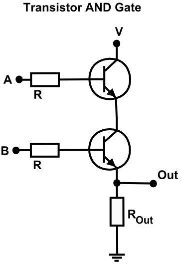 An implementation of a logical AND gate using transistors.
As you can see for the current to flow from V to Out both A and
B inputs must be high.
If we represent high voltages as 1s and low voltage levels as 0s we see that this circuit will create the logical-AND.
This is one way Boolean logic can be implemented in electronics. There are many other ways in which these logical operations can be implemented in circuitry, they can even be implemented mechanically although this approach doesn't scale (Unfortunately the economical effects of the poor scaling of mechanical computation probably stopped many inventions of the era of Babbage's Analytical engine by raising the cost of development beyond what a society that was unaware of the power of Turing-complete computing would be willing to pay).
Transistors
Essentially the transistor is a switch that allows a voltage to flow between two points if and only if a voltage is applied.
This lets us control one current path with another, which as you can see in the logic gate step before lets you construct the Boolean logic primitive operations required for computations.
(Note that your CPU of 201x era is likely using MOSFETs because of the properties of such components, including their ability to be miniaturized effectively.)
-
We are assuming x86 for the purposes of this article just because of how widespread it is at the time of the article being written, there are many other instruction sets that are used in the industry. ↩
By Janis Lesinskis
This post is part 7 of the "PageRequestsToTheMetal" series:
- Page requests to the metal - introduction
- Page requests to the metal - frontend
- Page requests to the metal - Network stack - From frontend to backend
- Page requests to the metal - Backend - What happens on the server
- Page requests to the metal - Backend web framework
- Page requests to the metal - Backend implementation
- Page requests to the metal - hardware level *